Skip to content

Instantly share code, notes, and snippets.

@stecman
Last active August 20, 2024 18:26
Show Gist options
  • Save stecman/f748abea0332be1e41640fd25b5ca861 to your computer and use it in GitHub Desktop.
Save stecman/f748abea0332be1e41640fd25b5ca861 to your computer and use it in GitHub Desktop.
STM8S code examples

This is a collection of code snippets for various features on the STM8S family microcontrollers (specifically the STM8S003F3). These are written against the STM8S/A SPL headers and compiled using SDCC.

Some of this controller's functions aren't particularly intuitive to program, so I'm dumping samples for future reference here. These are based on the STM8S documentation:

Run at 16MHz

// Configure the clock for maximum speed on the 16MHz HSI oscillator
// At startup the clock output is divided by 8
CLK->CKDIVR = 0x0;

PWM output using TIM1

Note that on the STM8S003F3, TIM1_CH1 output requires configuring an Alternate Pin Function (see next snippet).

const uint16_t tim1_prescaler = 0;
TIM1->PSCRH = (tim1_prescaler >> 8);
TIM1->PSCRL = (tim1_prescaler & 0xFF);

const uint16_t tim1_auto_reload = 16000; // 1KHz assuming at 16MHz clock
TIM1->ARRH = (tim1_auto_reload >> 8);
TIM1->ARRL = (tim1_auto_reload & 0xFF);

const uint16_t tim1_compare_reg1 = 4000; // 25% duty cycle
TIM1->CCR1H = (tim1_compare_reg1 >> 8);
TIM1->CCR1L = (tim1_compare_reg1 & 0xFF);

// Set up compare channel 1
TIM1->CCER1 = TIM1_CCER1_CC1E; // Enable compare channel 1 output
TIM1->CCMR1 = TIM1_OCMODE_PWM1; // Make OC1REF high when counter is less than CCR1 and low when higher

TIM1->EGR |= TIM1_EGR_UG; // Generate an update event to register new settings
TIM1->BKR = TIM1_BKR_MOE; // Enable TIM1 output channels
TIM1->CR1 = TIM1_CR1_CEN; // Enable the counter

Using alternate pin functions (APF)

Some pins on the STM8S003 series are marked as having an "alternate function after remap". These are only documented in the datasheet, with register description under Option bytes.

As option bytes are stored in eeprom, they're a little more involved to set than regular registers. Eeprom can be addressed directly for reading, but needs to be unlocked before it can be written.

Option bytes are intended to be programmed once when uploading code to the chip, but they can be changed "on the fly" as the datasheet mentions:

// Set a bit in the Alternate Function Register (AFR) to switch pin-mapping
// This is stored in flash and is not a directly writable register
{
    const uint32_t AFR_DATA_ADDRESS = 0x4803;
    const uint32_t AFR_REQUIRED_VALUE = 0x1; // Enable TIM1_CH1 pin

    const uint16_t valueAndComplement = FLASH_ReadOptionByte(AFR_DATA_ADDRESS);
    const uint8_t currentValue = valueAndComplement >> 8;

    // Update value if the current option byte is corrupt or the wrong value
    if (valueAndComplement == 0 || currentValue != AFR_REQUIRED_VALUE) {
        FLASH_Unlock(FLASH_MEMTYPE_DATA);
        FLASH_ProgramOptionByte(AFR_DATA_ADDRESS, AFR_REQUIRED_VALUE);
        FLASH_Lock(FLASH_MEMTYPE_DATA);
    }
}

This works in a pinch and avoids an extra programming step, but switching function repeatedly during run-time is probably a bad idea:

  • There's likely an endurance issue as each change is written to flash/eeprom (datasheet claims 100k writes).

  • Writing some of the option bytes requires two writes: one for the data and one for its complement. If a reset occurs between the two writes, the option bytes need to be reprogrammed before the SWIM interface can program the chip again (stm8flash and ST Visual Programmer can still program the option bytes in this state, but error when trying to program the main flash).

Blocking ADC read

// Set up ADC
ADC1->CSR |= ADC1_CHANNEL_4; // Select channel to read
ADC1->CR2 = ADC1_CR2_ALIGN; // Place LSB in lower register
ADC1->CR1 = ADC1_CR1_ADON; // Power on the ADC

// Trigger single conversion
// (Yes, you write a 1 to the register a second time to do this - super intuitive...)
ADC1->CR1 |= ADC1_CR1_ADON;

// Wait until conversion is done
while ((ADC1->CSR & ADC1_CSR_EOC) == 0);

// Clear done flag
ADC1->CSR &= ~ADC1_CSR_EOC;

// Load ADC reading (least-significant byte must be read first)
uint16_t result = ADC1->DRL;
result |= (ADC1->DRH << 8);

ADC conversions driven by TIM1

This uses TIM1's compare channel 1 to trigger ADC readings. This can be slightly simpler if TRGO is configured to trigger on timer reset instead.

void init_adc(void)
{
    // Configure ADC to do conversion on timer 1's TRGO event
    ADC1->CSR = ADC1_CSR_EOCIE | // Enable interrupt at end of conversion
                ADC1_CHANNEL_4; // Convert on ADC channel 4 (pin D3)

    ADC1->CR2 = ADC1_CR2_ALIGN | // Place LSB in lower register
                ADC1_CR2_EXTTRIG; // Start conversion on external event (TIM1 TRGO event)

    ADC1->CR1 = ADC1_PRESSEL_FCPU_D18 | // ADC @ fcpu/18
                ADC1_CR1_ADON; // Power on the ADC


    // Configure TIM1 to trigger ADC conversion automatically
    const uint16_t tim1_prescaler = 16000; // Prescale the 16MHz system clock to a 1ms tick
    TIM1->PSCRH = (tim1_prescaler >> 8);
    TIM1->PSCRL = (tim1_prescaler & 0xFF);

    const uint16_t tim1_auto_reload = 69; // Number of milliseconds to count to
    TIM1->ARRH = (tim1_auto_reload >> 8);
    TIM1->ARRL = (tim1_auto_reload & 0xFF);

    const uint16_t tim1_compare_reg1 = 1; // Create a 1ms OC1REF pulse (PWM1 mode)
    TIM1->CCR1H = (tim1_compare_reg1 >> 8);
    TIM1->CCR1L = (tim1_compare_reg1 & 0xFF);

    // Use capture-compare channel 1 to trigger ADC conversions
    // This doesn't have any affect on pin outputs as TIM1_CCER1_CC1E and TIM1_BKR_MOE are not set
    TIM1->CCMR1 = TIM1_OCMODE_PWM1; // Make OC1REF high when counter is less than CCR1 and low when higher
    TIM1->EGR = TIM1_EGR_CC1G; // Enable compare register 1 event
    TIM1->CR2 = TIM1_TRGOSOURCE_OC1REF; // Enable TRGO event on compare match

    TIM1->EGR |= TIM1_EGR_UG; // Generate an update event to register new settings

    TIM1->CR1 = TIM1_CR1_CEN; // Enable the counter
}

void adc_conversion_irq(void) __interrupt(ITC_IRQ_ADC1)
{
    // Clear the end of conversion bit so this interrupt can fire again
    ADC1->CSR &= ~ADC1_CSR_EOC;

    // Load ADC reading (least-significant byte must be read first)
    uint16_t result = ADC1->DRL;
    result |= (ADC1->DRH << 8);

    // Use result ...
}

Crude delay function

These assume the clock is running at 16MHz and ok for crude blocking timing.

void _delay_us(uint16_t microseconds) {
    TIM4->PSCR = TIM4_PRESCALER_1; // Set prescaler

    // Set count to approximately 1uS (clock/microseconds in 1 second)
    // The -1 adjusts for other runtime costs of this function
    TIM4->ARR = ((16000000L)/1000000) - 1;


    TIM4->CR1 = TIM4_CR1_CEN; // Enable counter

    for (; microseconds > 1; --microseconds) {
        while ((TIM4->SR1 & TIM4_SR1_UIF) == 0);

        // Clear overflow flag
        TIM4->SR1 &= ~TIM4_SR1_UIF;
    }
}

void _delay_ms(uint16_t milliseconds)
{
    while (milliseconds)
    {
        _delay_us(1000);
        milliseconds--;
    }
}

Pin change interrupt

void init(void)
{
    // Configure pin change interrupt on pin B4
    EXTI->CR1 |= 0x04; // Rising edge triggers interrupt
    GPIOB->DDR &= ~(1<<4); // Input mode
    GPIOB->CR1 |= (1<<4);  // Enable internal pull-up
    GPIOB->CR2 |= (1<<4);  // Interrupt enabled
}

void portb_pin_change_irq(void) __interrupt(ITC_IRQ_PORTB)
{
    // Do something...
}
@stecman
Copy link
Author

stecman commented Feb 8, 2021

@atochukwu0 - assuming you have a STM8S003F3P6:as used in cheap break-out boards (like this one), this gets you complementary outputs on pins C3 and C4 without dealing with the alternative function register (AFR) to remap pins:

#include "stm8s.h"

const uint16_t tim1_prescaler = 0;
const uint16_t tim1_auto_reload = 315; // 1KHz assuming at 16MHz clock (trimmed as 320 was around 800Hz off for me)

void tim1_set_compare(uint16_t compare)
{
    // Load compare value for channels 3 and 4
    const uint8_t highByte = (compare >> 8);
    const uint8_t lowByte = (compare & 0xFF);

    TIM1->CCR3H = highByte;
    TIM1->CCR3L = lowByte;

    TIM1->CCR4H = highByte;
    TIM1->CCR4L = lowByte;

    // These values are now in shadow registers. They won't take effect until
    // the next update event (UEV), which happens automatically when the timer
    // hits the auto-reload value and rolls over (assuming UDIS is not set in
    // TIM1_CR1 to disable this).
    //
    // It probably make sense to set UDIS while changing multiple compare registers
    // so a UEV can't occur between the updating of channel 3 and 4 and cause
    // unexpected behaviour.
}

void tim1_init()
{
    TIM1->PSCRH = (tim1_prescaler >> 8);
    TIM1->PSCRL = (tim1_prescaler & 0xFF);

    TIM1->ARRH = (tim1_auto_reload >> 8);
    TIM1->ARRL = (tim1_auto_reload & 0xFF);

    // Set up compare channel 3 and 4 180 degrees out of phase This uses two
    // extra compare channels rather than the dedicated complementary output mode
    // to avoid configuring alternative pin mappings as that increases complexity.

    TIM1->CCER2 = TIM1_CCER2_CC3E | TIM1_CCER2_CC4E; // Enable compare channels 3 and 4

    
    TIM1->CCMR3 = TIM1_OCMODE_PWM1 | // Channel 3 low when counter is less than CCR3, otherwise high
                  TIM1_CCMR_OCxPE; // Preload enable: require a UEV event to load new compare values
    TIM1->CCMR4 = TIM1_OCMODE_PWM2 | // Channel 4 high when counter is less than CCR4, otherwise low
                  TIM1_CCMR_OCxPE;

    TIM1->EGR |= TIM1_EGR_UG; // Generate an update event to register new settings
    TIM1->BKR = TIM1_BKR_MOE; // Enable TIM1 output channels
}

inline void tim1_start()
{
    TIM1->CR1 |= TIM1_CR1_CEN; // Enable the counter
}

inline void tim1_stop()
{
    TIM1->CR1 &= ~TIM1_CR1_CEN; // Disable the counter
}

int main(void)
{
    // Configure the clock for maximum speed on the 16MHz HSI oscillator
    // At startup the clock output is divided by 8
    CLK->CKDIVR = 0x0;

    int8_t direction = 1;
    uint16_t compare = tim1_auto_reload / 2;

    tim1_init();
    tim1_set_compare(compare);
    tim1_start();

    // Sweep duty cycle back and forward forever
    for (;;) {
        // Crude delay
        for (uint16_t i = 0; i < 0xFFF1; ++i) {
            nop();
        }

        compare += direction;

        if (compare == tim1_auto_reload) {
            direction = -1;
        } else if (compare == 0) {
            direction = 1;
        }

        tim1_set_compare(compare);
    }
}

That results in the following (though a lot slower than my slideshow of scope screenshots appears):

50KHz PWM changing duty-cycle stm8

@atochukwu0
Copy link

atochukwu0 commented Feb 8, 2021

Thank you very much for the example. if I may ask .
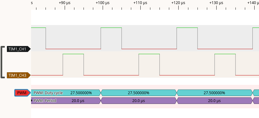
kfjckjmdcoodpcnn
This is low duty cycle .

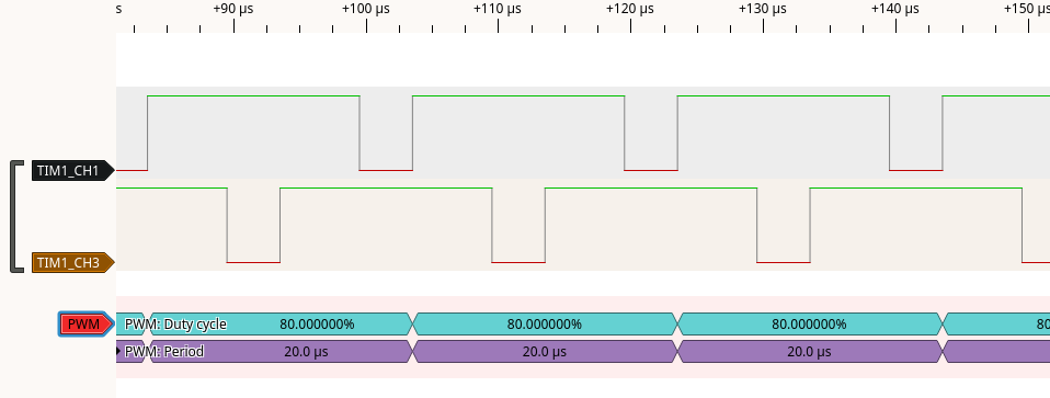
bgmmepcbkpnegmep
Also high duty cycle, this is exactly what I need , I don't know if the above example you provided will behave like pwm waveforms in above images ?.

@stecman
Copy link
Author

stecman commented Feb 8, 2021

Aha, thanks for the waveform @atochukwu0 - I had tunnel vision on the complementary output part. With the STM8S I think you'll need to use two timers to achieve this. Not ideal since there are only a few timers in these chips, but it's workable.

In the STM8S family there are two possible approaches:

  1. Run two timers with the same settings, starting both timers manually with one starting at 50% instead of 0.
  2. Run two timers with the same settings, configuring one timer to start the other after a precise delay using TRGO

Unfortunately option 2 isn't possible on the STM8S003F3P6 as it lacks TIM5 which is the only timer supporting start by TRGO event.

The following gets you PWM signals on pin C3 and D3, with the latter phase shifted by 180 degrees:

#include "stm8s.h"

const uint8_t timer_prescaler = 0;
const uint16_t timer_auto_reload = 315; // 1KHz assuming at 16MHz clock (trimmed as 320 was around 800Hz off for me)

void timer_set_compare(uint16_t compare)
{
    // Load compare value for channels 3 and 4
    const uint8_t highByte = (compare >> 8);
    const uint8_t lowByte = (compare & 0xFF);

    TIM1->CCR3H = highByte;
    TIM1->CCR3L = lowByte;

    TIM2->CCR2H = highByte;
    TIM2->CCR2L = lowByte;

    // These values are now in shadow registers. They won't take effect until
    // the next update event (UEV), which happens automatically when the timer
    // hits the auto-reload value and rolls over (assuming UDIS is not set in
    // TIM1_CR1 to disable this).
    //
    // It probably make sense to set UDIS while changing multiple compare registers
    // so a UEV can't occur between the updating of channel 3 and 4 and cause
    // unexpected behaviour.
}

void timer_init()
{
    // Configure timer 1
    //

    TIM1->PSCRH = 0; // Use a 4-bit prescaler to be compatible with TIM2
    TIM1->PSCRL = timer_prescaler;

    TIM1->ARRH = (timer_auto_reload >> 8);
    TIM1->ARRL = (timer_auto_reload & 0xFF);

    TIM1->CR1 |= TIM1_CR1_ARPE; // Buffer new timer auto-reload value rather than updating directly

    TIM1->CCER2 = TIM1_CCER2_CC3E; // Enable compare channel 3

    TIM1->CCMR3 = TIM1_OCMODE_PWM1 | // Channel 3 low when counter is less than CCR3, otherwise high
                  TIM1_CCMR_OCxPE; // Preload enable: require a UEV event to load new compare values

    TIM1->EGR |= TIM1_EGR_UG; // Generate an update event to register new settings
    TIM1->BKR = TIM1_BKR_MOE; // Enable TIM1 output channels

    // Configure timer 2
    //
    TIM2->CR1 |= TIM2_CR1_ARPE; // Buffer new timer auto-reload value rather than updating directly
    TIM2->PSCR = timer_prescaler; // Run with no prescaler

    TIM2->ARRH = (timer_auto_reload >> 8);
    TIM2->ARRL = (timer_auto_reload & 0xFF);

    TIM2->CCER1 = TIM2_CCER1_CC2E; // Enable compare channel 2

    TIM2->CCMR2 = TIM2_OCMODE_PWM1 | // Channel 2 low when counter is less than CCR3, otherwise high
                  TIM2_CCMR_OCxPE; // Preload enable: require a UEV event to load new compare values

    TIM2->EGR |= TIM2_EGR_UG; // Generate an update event to register new settings
}

inline void timer_start()
{
    // Start timer 1 at zero
    TIM1->CNTRH = 0;
    TIM1->CNTRL = 0;

    // Start timer 2 offset 180 degrees from timer 1
    const uint16_t offset = timer_auto_reload / 2;
    TIM2->CNTRH |= (offset >> 8);
    TIM2->CNTRL |= (offset & 0xFF);

    // Enable the counters
    TIM1->CR1 |= TIM1_CR1_CEN;
    TIM2->CR1 |= TIM2_CR1_CEN;
}

inline void timer_stop()
{
    // Disable the counters
    TIM1->CR1 &= ~TIM1_CR1_CEN;
    TIM2->CR1 &= ~TIM2_CR1_CEN;
}

int main(void)
{
    // Configure the clock for maximum speed on the 16MHz HSI oscillator
    // At startup the clock output is divided by 8
    CLK->CKDIVR = 0x0;

    int8_t direction = 1;
    uint16_t compare = timer_auto_reload / 2;

    timer_init();
    timer_set_compare(compare);
    timer_start();

    // Sweep duty cycle back and forward forever
    for (;;) {
        // Crude delay
        for (uint16_t i = 0; i < 0x833F; ++i) {
            nop();
        }

        compare += direction;

        if (compare == timer_auto_reload) {
            direction = -1;
        } else if (compare == 0) {
            direction = 1;
        }

        timer_set_compare(compare);
    }
}

This leaves you with just one 8-bit timer if you're on the same part as me, but it appears similar to the signal you're after:

50KHz STM8 PWM example phase shifted

If you need the waveform valleys and peaks centered like they appear in your screenshot, you'd need to adjust the offset dynamically I believe. Whoops, on further inspection they are already are centred...I was seeing things

@atochukwu0
Copy link

atochukwu0 commented Feb 8, 2021

Wooah, that's exactly what I need , thank you , I owe you a beer 🤩🤩🤩.

I'll choose STM8 with more number of timers (STM8S207K6).
If you don't mind providing the option 2 . For learning purposes .

But I will stick to option 1 to use on my projects .

@atochukwu0
Copy link

Though the signal am after was generated using only one timer, so I didn't know how possible it is .

@atochukwu0
Copy link

I guess similar approach can work for stm32 using bare metal configurations.

@stecman
Copy link
Author

stecman commented Feb 8, 2021

@atochukwu0 - is your reference from an STM8 chip, or something else? It's certainly possible on more advanced chips from other ranges and brands to do this with a single timer, but the STM8 range is fairly basic

@atochukwu0
Copy link

The user developed his own header files for stm8, but bare metal approach is my best choice so far . So he used STM8s105 for the reference.

@atochukwu0
Copy link

Please @stecman, can you show example of ADC2 trigger and scan mode, measuring 5 ADC channels . ADC2 . Please .

@wuschel-brompf
Copy link

wuschel-brompf commented Jul 13, 2021

awesome - the first person telling the source of their wisdom. Your snippets got me started, but the linked reference manual was exactly what I needed. Now that I have RM0016 (thanks to you), I see that it is referenced to in all product datasheets facepalm.

Thank you!

@stecman
Copy link
Author

stecman commented Aug 21, 2021

ADC2 trigger and scan mode, measuring 5 ADC channels

@atochukwu0 page 428 in the the reference manual lists "scan mode for single and continuous conversion" as a feature only available on ADC1. ADC2 is simpler and lacks the output buffer that allows for ADC1's scan mode. To achieve the scan behaviour on a part that only has ADC2, you'd need to implement it in software.

What part are you using, out of curiosity? None of the STM8 parts I have on hand have ADC2, so I can't test any example code for this case.

@atochukwu0
Copy link

L

ADC2 trigger and scan mode, measuring 5 ADC channels

@atochukwu0 page 428 in the the reference manual lists "scan mode for single and continuous conversion" as a feature only available on ADC1. ADC2 is simpler and lacks the output buffer that allows for ADC1's scan mode. To achieve the scan behaviour on a part that only has ADC2, you'd need to implement it in software.

What part are you using, out of curiosity? None of the STM8 parts I have on hand have ADC2, so I can't test any example code for this case.

Am using STM8S207K8

@Benedito821
Copy link

Benedito821 commented Jul 3, 2023

This is a really good note . One of these particularities made me spend too much time to move forward on some projects. Regarding to the option bytes, a handier way of managing them (for those who use the IAR IDE) is to downloading the code, running the debugging , going to the menu ST_LINK, then option bytes... . A window is going to pop up and we can chose the needed alternate function, right-mouse click it and switch to Alternate active (for option bytes AFR0-AFR7).

@sahasradal
Copy link

Dear Sir,
I am trying to test the trigger standard mode , trigger reset mode and gated trigger mode on stm8S103 TSSOP20 version. I initialized the registers as described in RM0016 manual . The Timer1 counter keeps on counting on its own and doesnt wait for the trigger to happen on TI1 or TI2 inputs (PC6 & PC7). The AFRO0 option byte was enabled to make timer1 chanel 1 and chanel 2 available. Request help form informed members on how to realise the trigger modes. Please find below the code I used. I have used the TIMER1 _ chanel2 as input and timer1 overflow interrupt to toggle an led on PD4. The led is supposed to toggle when the PC7 goes high but I see the LED toggles when power is applied to the chip even when PC7 is supplied ground. Below code is to test trigger standard mode. Any help to make this work is highly appreciated.
Regards
Sajeev

main_loop.l:
mov CLK_CKDIVR,#$00 ; cpu clock no divisor = 16mhz
bset PD_DDR,#4 ; set PD4 as output
bset PD_CR1,#4 ; set PD4 as pushpull
timer_setup:
bres TIM1_CR1,#0 ; disable timer
bres TIM1_SR1,#0 ; clear update interrupt flag
mov TIM1_SMCR,#$66 ; TS = 110 and SMS = 110 , TI2 input , trigger standard mode
bset TIM1_IER,#0 ; enable update interrupt
bset TIM1_CR1,#0 ; enable timer
RIM

wait
jra wait

interrupt TIM1_ISR
TIM1_ISR
bres TIM1_SR1,#0 ; clear interrupt flag
bcpl PD_ODR,#4 ;toggle led pin
iret

@sahasradal
Copy link

Dear Sir,
I found my mistake. I shouldn't be enabling CEN bit in CR1 register. Once that line ("bset TIM1_CR1,#0 ; enable timer ")was removed the trigger standard mode works fine. the counter starts counting only on receiving a high on TI2 PC7.
Thanks
Sajeev

Sign up for free to join this conversation on GitHub. Already have an account? Sign in to comment