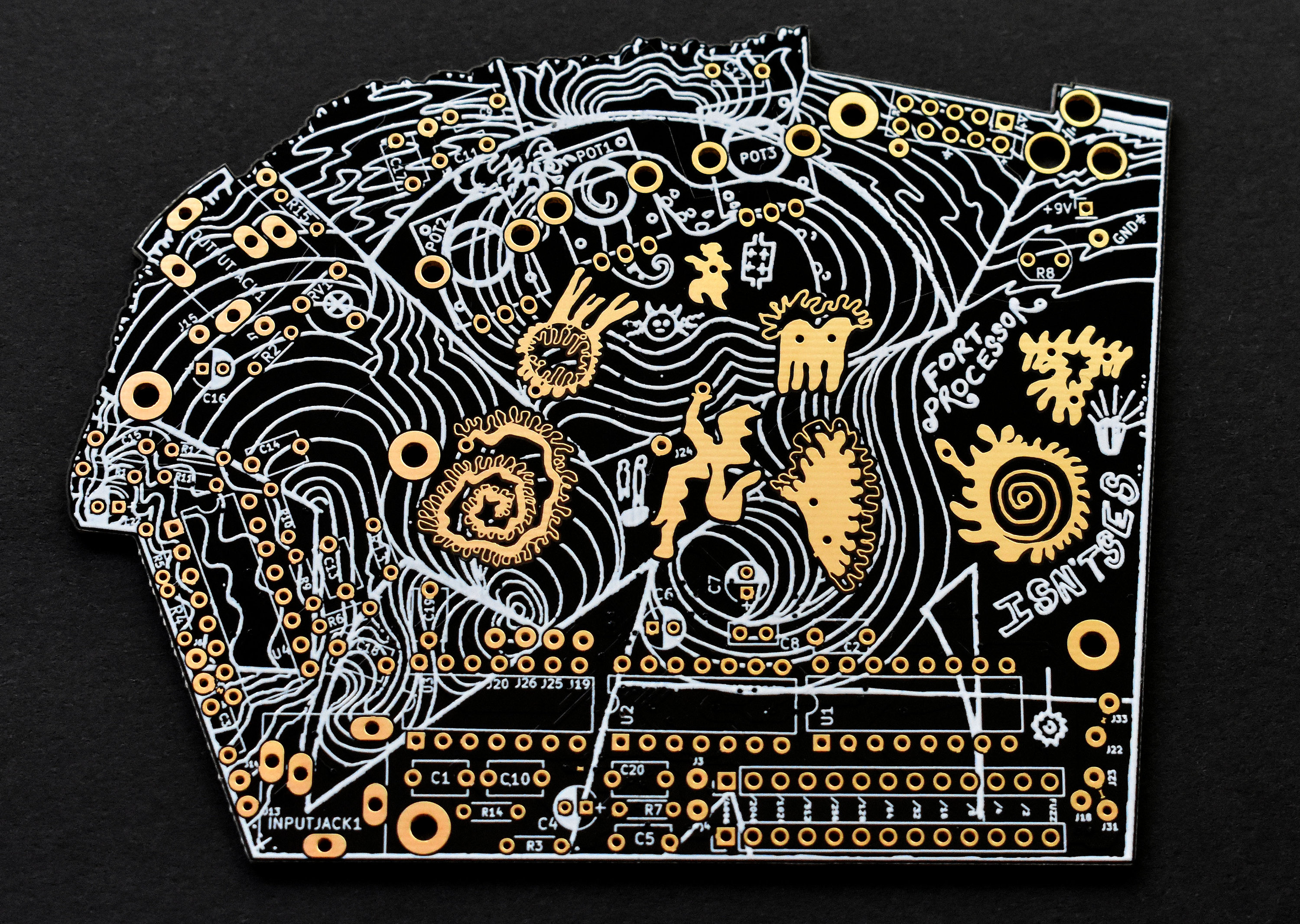
Disclaimer: I have zero background in electrical engineering; this here is my attempt to summarize what I've learned while creating my first PCB, which ended up not having any components on it. I set myself a simple goal: create a PCB that's an animal, and when you click a button, the eyes (LEDs) light up. I ended up in a slightly different path, and I ended up ordering a cat shaped PCB where the eyes are gold plated.
Key points:
- I was inspired by things like: https://i.etsystatic.com/21566051/r/il/2d8ef5/2541130934/il_fullxfull.2541130934_imkt.jpg and https://images.goodsmile.info/cgm/images/product/20200923/10116/79405/large/a4c976b8804781ccccf2ade0636fdb56.jpg
- I wanted to learn how to achieve the estetic of black board (solder mask), white print (silkscreen) and golden details (gold plated copper)
- (warning) I'm in the process of ordering, so no idea if it'll turn out like I expect it
- Important layers: F.Cu (copper), F.Mask (solder mask), F.Silkscreen, Edge.Cuts (outline)
- install KiCad and Inkscape
- find an image; it takes a bit of trial and error to understand what kind of image works well; in my case, for a cat, I ended up using: http://wallpapercave.com/wp/ePMeSmp.jpg
- it has a white background, it has contrast, and the eyes are perfect for the golden highlights
- import image into Inkscape and do "Trace Bitmap"
- what you're aiming for is to export three files:
- outline: which you'll export as .svg and then convert to .dxf
- silkscreen: which is the traced bitmap, INVERTED
- gold: which you'll import into BOTH F.Cu (copper) and F.Mask (solder mask)
- an important things to understand: the silkscreen layer MUST NOT overlap the F.Cu layer, since you obviously can't print directly over copper
- you solve this in Inkscape by subtracting the gold layer path, from the silkscreen path
- do this by selecting the gold shape and the silkscreen shape, and do Path -> Difference
- you'll notice that the "Difference" action deletes the gold path, so Undo, duplicate (ctrl+D), and subtract again
- now a new problem arises: the hole in the silkscreen should be BIGGER than the gold shapes, so go back again, do Duplicate, then Path -> Outset, Difference and you'll probably end up with a hole in the silkscreen which the golden shapes fit nicely
- export the outline into an .svg file and convert it to .dxf using: https://cloudconvert.com/svg-to-dxf
- export the silkscreen into an .svg
- if KiCad crashes on import, the shape might be to complex -- if that's the case, do Path -> Simplify in Inkscape
- export the gold layer
- you'll import the same layer into F.Cu and F.Mask, because you want the copper to be shaped in the same way that the solder mask is cut
- i have yet to see if making them exactly the same is a problem, or we need to leave some margin around the copper
- in KiCad, start a new project
- first do File -> Import Graphic, choose the "Edge.Cuts" layer and import the .DXF file (NOT THE SVG)
- check with the 3D viewer (alt+3) that it renders it in the correct shape
- next, import the silkscreen .svg graphic onto the F.Silkscreen layer -- if it crashes, simplify the shape in Inkscape using Path -> Simplify
- make sure to choose some adequate snap-to-grid option, because here you need perfect alignment of the layers, for the next step
- import the gold .svg graphic in the F.Cu layer
- import the gold .svg graphic in the F.Mask layer, and make sure the PERFECTLY overlap
- run Inspect -> Design Rules Checker (you should get 0 errors/warnings)
- File -> Fabrication Outputs -> Gerbers
- generate drill files as well
- zip all gerbers (including drill files) and upload the zip to JLCPCB or PCBWay
- if the small preview is wrong, try logging in and using the more advanced Gerber viewer
If you end up on this gist by googling stuff and you're desperate, feel free to contact me on my email: first name plus last name, no spaces, at gmail :)
Here's what I ended up ordering:
